- The control power is null, that is to say, current by the control terminal is not absorbed.
- A very weak signal can control the device.
- The control tension is used to create an electric field.
There are two families of transistors of field effect: the JFET and the MOSFET. Although the basic concept of the FET was known already in 1930, these devices only began to make commercially as of the decade of the 60. And from the 80 transistors of type MOSFET they have reached an enormous popularity. Compared with the BJT, transistors MOS they occupy less space, that is to say, within an integrated circuit it can incorporated I number greater. In addition its process to manufacture is also simpler. In addition, a great number of functions exists logics that can solely be implemented with transistors MOS (without resistance nor diodes). This has made of transistor MOS the component star of the digital electronics.
In this chapter the principle of operation of both types of devices, as well as their elementary circuitales models is explained.
TRANSISTOR OF EFFECT OF UNION FIELD (JFET)
A JFET of channel N makes spreading a region of P type in a channel of N type, so and as it is in Figure 1. To both sides of the channel the terminals of source (S, S ource)anddrainage are connected (D, Drain). The third terminal denominates door (G, Gate).
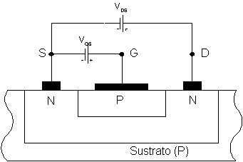
Figure 1: Scheme of transistor JFET of channel N
The symbols of this type of devices are:
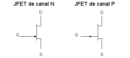
Figure 2: Symbols of transistors JFET
The explanations including in this chapter talk about fundamentally to transistor NJFET, considering that the principle of operation of the PJFET is analogous.
PRINCIPLE OF OPERATION OF THE NJFET
Next it is explained how the current in a JFET is controlled. Like the JFET happens to transistors BJT it has three regions of operation:
- Region of cut
- Linear region
- Region of saturation
It is precise to make notice that in this case, the saturation alludes to a phenomenon completely different from the one from transistors BJT.
Region of cut
Let us focus our attention on Figure 1. The zone of P type connected to the door forms a diode with the channel, that is of N type. As one will remember, when a union PN forms appear in the edges of same a zone of deplección in which there are no free carriers of load. The width of this zone depends on the applied polarization. If this is inverse, the zone becomes wider, proportionally to the applied tension. Applying a negative tensionV GS we increased the width of the zone of deplección, with which the width of conduction diminishes channel N.
If the value of VGS becomes the sufficiently negative thing, the exhaustion region will extend completely through the channel, of which the resistance of the same one will take control infinite and the passage of I D will be prevented (Figure 3). The potential to which east phenomenon happens denominates potential of blockade (Pinch Voltage, VP).
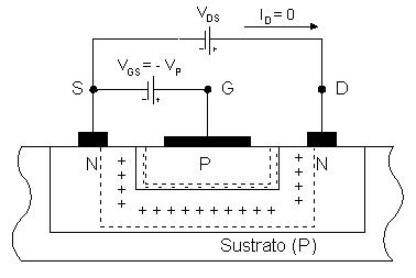
Figure 3: Scheme of transistor JFET of channel N polarized with the tension of blockade
Therefore, for values more negative than VP transistor NJFET is polarized in the cut region, and the drainage current turns out to be null.
Linear region
If in the structure of Figure 1 a tension V DS is applied greater than zero, will appear a current circulating in the sense of the drainage to the source, current that we will call ID. The value of current happiness will be limited by the resistance of conduction channel N. In this case two situations can be distinguished according to is greator small V DS in comparison with VGS.
Small values of the voltage drainage-source
Figure 4 presents/displays the situation that is obtained when union GS with a negative tension is polarized, whereas a tension between smaller D and S is applied.
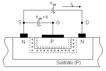
Figure 4: Scheme of transistor JFET of channel N polarized with VGS < 0
Around the terminal of door (g) it does not circulate more than the current of flight of the diode GS, that in one first approach we can consider despicable. Current ID presents/displays one double dependency:
- Current ID is directly proportional to the value of VDS
- The width of the channel is proportional to the difference between VGS and VP. As ID is limited by the resistance of the channel, whichever greater it is VGS - VP, greater it will be the width of the channel, and greater the obtained current.
Both previous points take shelter in the following expression:

Therefore, in the linear region we directly obtain a proportional current to VGS and VDS.
High values of the voltage drainage-source
For values of VDS comparable and superior to VGS the situation changes with respect to the previous case: the resistance of the channel becomes nonlinear, and the JFET loses their ohmic behavior. Let us see why this happens.
When a voltage V DS is applied to the channel of 5 volts, for example, this it is distributed throughout the channel, that is to say, in the proximities of terminal D the tension will be of 5 V, but halfway the circulating current will have reduced its potential to half (2.5 V), and in the terminal S the potential will be null. On the other hand, if VGS is negative (- 2 V, for example), the tension will be distributed uniformly throughout the P zone, when not existing no current (Figure 5). (NOTE: the fall of tension in the zones located below the contacts not deigns).
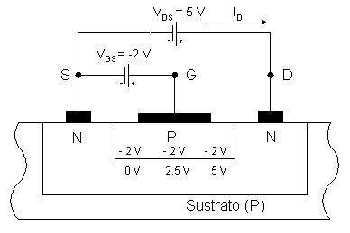
Figure 5: Scheme of transistor JFET of channel N polarized with VGS = -2 5 V andV DS = V
Let us follow ahead. In the proximities of the terminal S the applied inverse tension is of 2 V, that corresponds with VGS = -2 V. , nevertheless in agreement we approached D this tension increases: in half of the channel V is of 4.5, and in 7 D V reaches. The inverse polarization applied to the channel is not constant, with which the width of the zone of deplección will not be it either (Figure 6). When VDS is small, this difference of widths does not affect to the conduction in the channel, but when it increases, the variation of the conduction section causes that the drainage current is a function nonlinear of VDS, and that diminishes with respect to the obtained one without considering east effect.
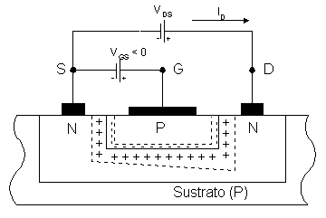
Figure 6: Scheme of transistor JFET of channel N in the region of conduction nonlinear
Region of saturation
If VDS is increased more, it will be arrived at a point where the thickness of the channel in the end of the drainage approaches zero. As of that moment, the current stays independent of VDS, since the increases of tension cause a greater narrowing of the channel, with which the global resistance increases (Figure 7).
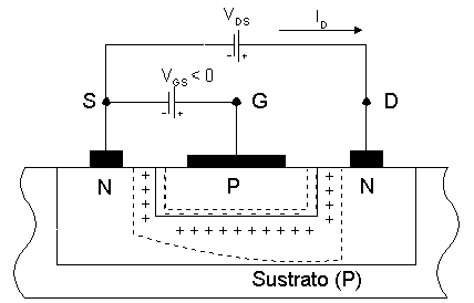
Figure 7: Scheme of transistor JFET of channel N in the region of constant current
The saturation region occurs when the channel in the drainage strangles, which happens when the tension door-drainage is more negative than VP, is to say:
VGD < VP = > VGS - VDS < VP = > VDS > VGS - VP
Before following ahead, we compare the figures 3 Figure and Figure 7. In the case of the blockade, all the channel is affected by the zone from deplección, that is constant because tension VGS is applied uniformly throughout the union. However, in the region of constant current only part of the channel has arrived at the blockade (caused by VDS, that varies throughout the same one), and it is what the circulation of the current allows.
1.2 CURVED CHARACTERISTICS
They are the two curves that are handled habitually to characterize transistors JFET. In the first place, in the representation of ID as opposed to VGS, for a givenV DS, the passage of the region of cut to the one of saturation is appraised clearly (Figure 8). Actually only one operates in the second quadrant of the graph, since first positiveV GS lets grow I Gquickly.
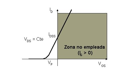
Figure 8: Characteristic VGS - ID of transistor NJFET
In characteristic VDS - ID of transistor NJFET is observed the difference between the regions linear and of saturation (Figure 9). In the linear region, for a determined VGS, the current it grows proportionally to tension VDS. Nevertheless, this growth is attenuated until getting to be null: the value of saturation is reached, in where Ionly D depends on VGS.
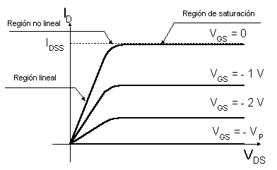
Figure 9: Characteristic VDS - ID of transistor NJFET
Nótese that, according to this graph, the region of saturation of the JFET is identified with the normal active region of the bipolar transistors. Whereas in RAN the collector current only depends on the one of base, here the magnitude of control is tension VGS. On the contrary, if the resistance of the JFET in the linear region is very small can be a certain parallelism between the regions linear of JFET and saturation of the BJT.
1,3 COMMERCIAL PARAMETROS
One appears next some of the characteristics of the transistors JFET that offer the manufacturers in the data sheets:
- IDSS: It is the drainage current when transistor JFET is in configuration of common source and cortocircuita the door and the source (VGS= 0). Actually it marks to the Maxima intensity that can circulate around the transistor. It agrees to consider that transistors JFET present/display ample dispersions in this value.
- VP (Pinch-Off Voltage): it is the tension of strangling of the channel. Like IDSS, presents/displays forts dispersions in their value.
- RDS(ON): He is inverse of the slope of curve ID/VDS in the linear zone. This value stays constant until values of VGD near the strangling tension.
- BYOU (Drain-Source Breakdown Voltage): it is the tension of rupture between source and drainage. Tensions higher than BYOU cause a fort increase of ID.
- BVGS (Gate-Source Breakdown Voltage): it is the tension of rupture of the union between the door and the source, that is polarized in inverse. Greater values of BVGS cause a conduction by avalanche of the union.
1,4 MODELS OF TRANSISTOR NJFET
Analogous to the carried out thing with the bipolar transistor they are going away to present/display two models for the JFET: one to analyze the operation of the transistor JFET with continuous signals and another one for the applied alternating signals on a point of operation of the saturation region.
In the first place the models for the different regions from operation appear, that is to say, cuts, saturation and linear zone. To start off of the equations dictated by this model, the necessary expressions for the analysis of signals of alternating are deduced later of small amplitude.
1.4.1 Ideal static model
For transistor NJFET, the model it comes represented in Figure 10. The value of ID depends on the operation region of the transistor.
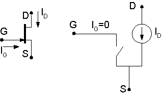
Figure 10: Circuital scheme of the model of transistor JFET
- Region of cut: the condition of the cut region is that the channel completely is strangled in the proximities of the source, which happens when the tension door-source reaches the strangling tension (VGS< VP). In this case ID= 0.
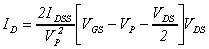
- Linear region: it is the region in which an increase of intensity I D when increasing V DS takes place. This increase is linear for low values of VDS although the linearity is lost when VDS approaches - VP. In order to work in the linear region two conditions are due to give:
- VGS > VP
- VGD > VP VGS > VP + VDS
These conditions are equivalent to admit that the conduction channel does not strangle as much by the zone of deplección in inverse in the end of drainage like in the source. The value that takes current ID is
- Region of saturation: the saturation region takes place when the tension between drenador and door reaches the strangling tension. So that it happens, channel N, must be strangled in the end near the drainage, but not in the end of the channel near the source. Then, like in the previous case, two conditions must happen:
- VGS > VP
- VGD < VP VGS < VP + VDS
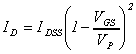
In this case intensity ID no longer depends on VDS, being its expression
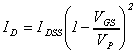
Generally, in transistors NJFET as much VP as VGS they take negative values, whereas VDS and IDSS is positive, taking direction ID so and as it appears in the model.
1.4.2 Model for alternating signals
For the deduction of the same one the following hypotheses are considered:
- Transistor polarized in the saturation region
- Alternating oscillations of low amplitude and LF
1.4.2.1 General expressions
Of between the diverse possible options, for the deduction of the model tensions V GS and V DS are chosenlike independent variables, whereas the employees are currents IG and ID. This way, the equations characteristic of the transistor will come given by two functions f1 and f2 such that:
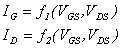
The tensions and currents of a concrete point of polarization will come given by the previous expressions:
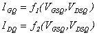
Let us suppose that on this point of operation Q an alternating component is added, characterized by a VGS and a VDS. The oscillations of the currents can calculate like:
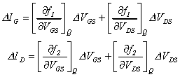
As of this moment, to simplify the annotation the increases of the variables will be written with very small letter. The previous expression admits a matrix representation:
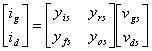
in where the coefficients andij are called parameters admittance.
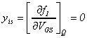
- andis : Admittance of entrance (-1)
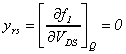
- andRS: Admittance of inverse transference (-1)
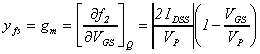
- andfs : Transconductancia (-1). Usually one names like gm
- andyou : Admittance of exit (-1)
1.4.2.2 Calculation of the parameters admittance
For the calculation of the parameters andij they are going away to use the resulting expressions of the static model for the saturation region.
- Function f1 = >

- Function f2 = >
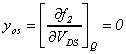
The circuital representation of this simplified model responds to the same scheme presented/displayed in Figure 10.
2 TRANSISTOR MOSFET
The benefits of transistor MOSFET are similar to those of the JFET, although their principle of operation and its internal structure are different. Four types of transistors MOS exist:
- Enrichment of channel N
- Enrichment of P channel
- Impoverishment of channel N
- Impoverishment of P channel
The symbols are:
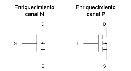
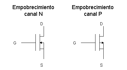
Figure 11: Transistors MOSFET
The common constructive characteristic to all the types of transistor MOS is that the terminal of door (g) is formed by a structure of Metal/Óxido/Semiconductor type. The oxide is insulating, with which the door current is practically null, much smaller than in the JFET. For that reason, the MOS is used to deal with signals very low power.
2,1 OPERATION PRINCIPLE
Of between all the types of existing transistors MOS one is going away to analyze the principle of operation of two of them: the NMOS of enrichment and impoverishment.
2.1.1 NMOS of enrichment
In Figure 12 the scheme of a MOS of enrichment appears channel N.
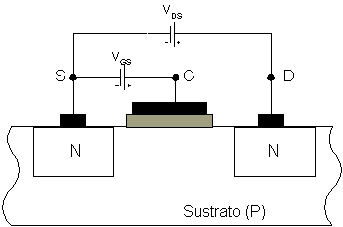
Figure 12: Scheme of enrichment transistor NMOS
Let us suppose that a tension V DS is applied greater than zero whereas VGS stays in zero. When applying a positive tension to zone N of the drainage, the diode that forms this one with the P substrate will polarize in inverse, with which the current passage will not be allowed: the MOS will be in cut.
Let us continue supposing, and we think now that we applied a positive potentialV GS, while we also maintain V DS positive. The layer of insulator of the door is very thin, as much that it allows the positive potential applied to repel to the hollows and to attract electrons of the P. material To greater applied potential, greater number of electrons will be attracted, and greater number of hollows repelled. The consequence of this movement of loads is that underneath the terminal G a negative channel is created, of N type, that puts in contact the drainage with the source. Around this channel a current can circulate. Summarizing, over a positive value VGS = VTH makes possible the circulation of current ID (Figure 13). We were before a region of linear conduction.
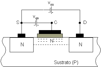
Figure 13: Scheme of transistor NMOS of enrichment in conduction
If the value of VDS increases, the effective tension on the channel in the proximities of the drainage (VGS - VDS) is diminishing, with which the channel is narrowed in this zone, and the linearity in relation I D is lost - VDS. Finally it is arrived at a situation of saturation similar to which is obtained in the case of the JFET.
2.1.2 NMOS of impoverishment
In Figure 14 the scheme of a MOS of impoverishment appears channel N.
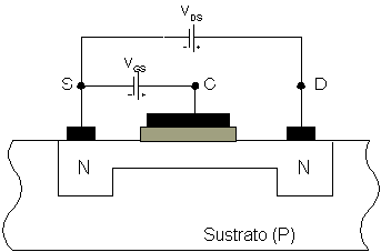
Figure 14: Scheme of impoverishment transistor NMOS
In this case the channel already is created. Therefore, if with VGS = 0 we applied a tension VDS will appear a current of drainage ID. So that the transistor happens to the cut state will be necessary to apply a tension VGS smaller than zero, than it expels to electrons of the channel.
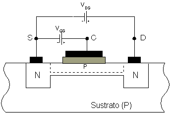
Figure 15: Scheme of transistor NMOS of impoverishment in cut
Also in this case, the application of a VDS much greater than VGS causes a situation of independendiente current of VDS.
2.2 CURVED CHARACTERISTICS
With transistors MOS two types of graphs are handled: characteristic VGS - ID, with constantV DS, and VDS - ID with constantV GS.
2.2.1 Transistor NMOS of enrichment
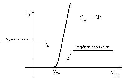
Figure 16: Characteristic VGS - ID of enrichment transistor NMOS
In Figure 16 it is shown how intensity ID increases abruptly when surpasses the tension threshold VTH (Threshold Voltage) and the channel is created. It is a suitable component for commutation, since it happens of a cut state to one of conduction from a value of the control signal. In the devices with the terminal of aluminum door and the silicon oxide insulator, the tension threshold is around the five volts.
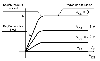
Figure 17: Characteristic VDS - ID of enrichment transistor NMOS
Characteristic VDS - ID of enrichment transistor NMOS is very similar to the one of the JFET, but the values of VGS change: in this case the conduction occurs for positive voltages over the threshold.
2.2.2 Transistor NMOS of impoverishment
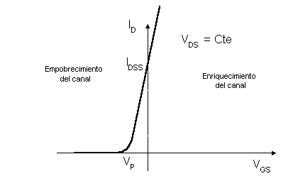
Figure 18: Characteristic VGS - ID of enrichment transistor NMOS
The NMOS of impoverishment can also work like enrichment transistor. If tension VGS becomes positive they will attract electrons the channel. In addition, unlike the JFET, the impedance of continuous entrance very being elevated.
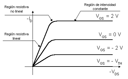
Figure 19: Characteristic VDS - ID of impoverishment transistor NMOS
2,3 COMMERCIAL PARAMETROS
The more important commercial parameters of transistor MOS are analogous to those of the JFET presented/displayed in section 1.3.
2,4 MODELS CIRCUITALES
So and as it has been seen, the curves of operation of transistors MOS are similar to those of the JFET. For that reason, all admit an analogous circuital representation.
2.4.1 Static model of Schichman-Hodges
The static model of transistor MOSFET denominates model of Schichman-Hodges. It is a model very similar to the model of transistors JFET, described previously. The equivalent circuit is made up of an open switch and a source of intensity (Figure 20) whose value ID depends on the operation region of the transistor.
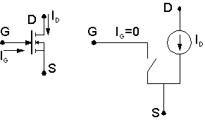
Figure 20: Model of Schichman-Hodges for transistor FETMOS
For enrichment transistor NMOS the operation regions are:
- Region of cut
- Condition VGS< VTH
- Intensity ID= 0
- Linear region.
- Conditions: VGS> VTH
VGD < VTH VGS < VTH+VDS
- Intensity:
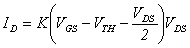
Where K is a constant that depends on the material and the dimensions of the transistor
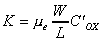
- mand is the mobility of the electrons, that depends on the material and the temperature
- W, Ls are the width and the length of the channel. Geometric factors that depend on the design of the transistor.
- C'OX is the capacity by unit of surface of the condenser that forms the metal of the door with the channel. It depends strongly on the thickness of door oxide.
- Region of saturation
- Conditions VGS > VTH
VGD > VTH VGS > VTH+VDS
- Intensity:
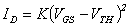
2.4.2 Model for alternating signals
For the case in which the transistor has supported to alternating signals of small amplitude and LF on a point of polarization in saturation region, it can be demonstrated of analogous form to since it has been made for the transistor JFET that transconductancia gm calculates through the following expression

3 APPLICATIONS OF THE TRANSISTORS OF FIELD EFFECT
The general applications of all the FET are:
3,1 ELECTRONICA ANALOGICA
For these applications of they use prepared transistors to lead great currents and to support high tensions in cut state.
- Variable resistors of governable value by tension (varying the width of the channel).
- Amplifiers of tension, specially in the initial amplification of signals of very low power.
- Control of electrical power given one loads.
In the case of the amplification the circuits are designed so that the point of operation DC of the MOS is in the saturation region. This way a current of dependent drainage only of tension V GS is obtained.
3,2 DIGITAL ELECTRONICA
The MOS is often used in digital electronics, due to the capacity to work between two states differentiated (cuts and conduction) and to his under consumption from control power. For this application devices of very low resistance are used, ideally so that it can be considered that:
- The fall of tension in conduction is very small.
- The transition between the state of cut and the one of conduction is instantaneous.
- In a transistor NJFET with IDSS= 10mA and VP = - 5 V is moderate an intensity of drainage ID = 1mA. To find how much it is worth tension VGS if one admits that it works in the saturation region. To find the tension of feeding and minim so that the transistor works in saturation.
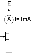
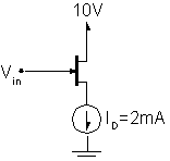
- In the circuit of the figure, it is requested:
1. - Tension VGS if one admits that the transistor is in saturation.
2. - If VIN = 5V, to calculate whichever bond VDS.
Data of the transistor: IDSS = 5mA; VP= - 3V
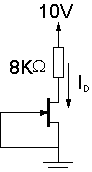
- Be the circuit of the figure formed by a transistor NJFET and a resistance. It is requested:
1. - To indicate the region of operation of the transistor.
2. - To calculate the point of operation of the transistor.
3. - If 1k changes to the resistance by another one of value, to find the new point of operation of the transistor.
Data of the transistor: IDSS = 2mA; VP= - 3V
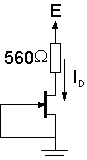
- Transistor NJFET of the figure has an IDSS= 12mA and VP= - 4V. To determine the minimum value of and so that the transitor works in the saturation region.
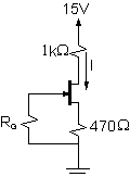
- To calculate the values of VDS and VGS of the transistor of the figure if I D is admittedthat= 5mA.
- To determine the point of operation of transistor FET of the figure supposing that one is in zone of saturation.
Data: IDSS= 5mA VP= - 4V
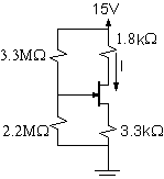
- To find the point of operation of the transistor of the figure. Data: IDSS= 15mA; VP= - 10V
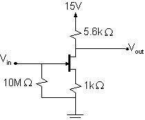
- In the circuit of the figure, to calculate the resistance of entrance RIN and the tension of exit VOUT. If a resistance of 4.7k of the circuit is connected when coming out, to calculate the exit tension. Data of the transistor: IDSS= 8mA, VP= - 10V
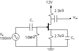
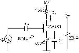
- In the circuit of the figure a transistor has been used 2N5460. To calculate the gain of tension of the circuit. Note: To use for it the average values of the parameters of the transistor.
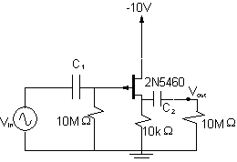
- To determine the gain of tension of the circuit of the figure. Data of the transistor: gm= 3,8 mmhos
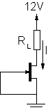
- The simple circuit of the figure is a current source that feeds a load RL.
a) Calcúlese the value of the current I that circulates around that load if the transistor is in the saturation region.
b) To find the resistance RL Maxima that can be fed with the intensity found by means of the previous circuit
If transistor JFET of the figure is a commercial transistor 2N5486, to calculate between what values can be hoped that it varies intensity I when the transistor works in the saturation region. Data: Idss= 10mA; VP= - 5V.
- With the transistor 2N5457 and other components that create necessary, designs a source of constant current of 0.2mA. Which will be the fully factored load that can feed the source on current?
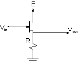
- In the circuit of the figure, to calculate the exit tension if the entrance tension is 3V. To consider that the transistor works in the saturation region. Additional data: R=100K; E=15V
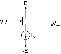
- The tension of entrance Vin is a tension that varies very slowly with time so that, the circuit by means of an analysis in continuous can be solved. If E=10V and ID= 1mA, to calculate the relation between Vout and Vin. What intensity ID is due to establish in the source if V is wanted thatout= Vin? Data of the transistor: IDSS= 3mA VP= - 5V
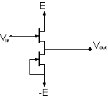
- In the circuit of the figure, if both transistors are identical and are thermally connections. To find the relation between VOUT and VIN.
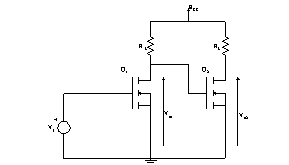
- To determine the value of 01 exitsV and V02 when VIN is worth zero and ten volts. Data: 5V TH = 20 V.And CC = V.
- For the design of an investing logical door, a scheme is made like which it imagines next.
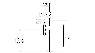
a) Approximately to calculate the power generated in the source of 8 Volts in the logical states ' 1' and ' 0 ' of the entrance (10 V. and 0 V. Respectivamente).
b) What mission has the resistance of 15 k.
- The following logic circuit is designed according to technique CMOS (Complementary-MOS).
It is denominated thus so that it uses in the same circuit transistors NMOS and PMOS.
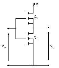
a) To explain its operation and to determine what type of logical door is.
b) To compare this circuit with the one of the previous one. What advantages present/display as far as power consumption.
- To select the most appropriate transistor for the following logic circuit (0 < VIN < 10V) (To calculate the commercial parameters of the transistor):
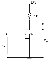
- To determine to what type of logical door corresponds the devices of the figure (Entered: V1 and V2; Exit: VOr)
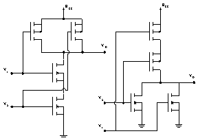
What power consumption has in states logical ' 1 ' and ' 0 ' of both circuits?
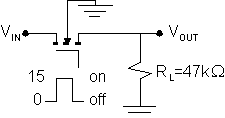
- The circuit of the figure represents a transistor acting like a switch. When the door with a tension of 15V is polarized, the transistor lets pass a current to feed the resistance on load. When polarizing with 0V the door, the transistor remains in cut. It is requested:
a) To choose an suitable transistor MOS to make this function.
b) Approximately to calculate the power loss in the transistor if the entrance signal is included/understood between 0 and 5V.
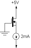
- A deplección transistor NMOS has a VP= - 2V and K=2mA/V2. To calculate minimumV DS to operate in the saturation region if VGS= 1V.
- Transistor MOSFET of deplección of the figure has a 2K=4mA/V and VP= - 2V. To calculate the tension of the source
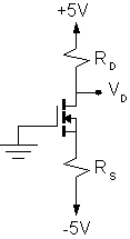
- To calculate the parameters that take resistance RD and RS from the circuit of the figure so that the transistor operates with an ID= 0.4mA and V1.DatosD =: VTH= 2V; K=0.4mA/V2
- It is desired to design an alarm circuit for a car so that when leaving the car with the ignited lights, it sounds a buzzer. In order to detect the opening of the door one has a magnetic sensor between the door and the car that is closed with the door and signals of 0V. When opening the door, the sensor signals of 5V. On the other hand, a device is had that detects the passage of current in the circuit of illumination. A signal of 5V with the ignited lights and 0V with the dull lights is obtained. The buzzer must be fed between 1 and 16V and to receive a current of 30mA. Design the circuit with necessary transistors MOSFET.


