Tiristores
INTRODUCTION:
A tiristor is one of the most important types of the semiconductor devices of power. The tiristores are used in extensive form in the electronic circuits of power. They operate like bistable commutators, passing of a state nonconductor to a conductive state. For many applications it is possible to be supposed that the Tiristores is interrupting or ideal commutators, although the practical tiristores exhibit certain characteristics and limitations.
CHARACTERISTIC OF THE TIRISTORS:
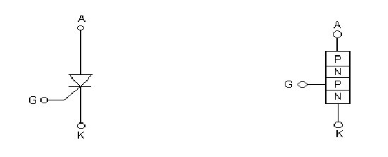
A Tiristor is semiconductor device of four layers of structure pnpn with three unions pn has three terminals: anode cathode and floodgate. Fig 1 shows to the symbol of the tiristor and a straight section of three unions pn. The tiristores make by diffusion.
When the voltage of the anode becomes positive with respect to the cathode, the unions J1 and J3 have direct or positive polarization. The J2 union has inverse polarization, and single a small current of flight of the anode to the cathode will flow. One says then that the tiristor is in direct condition of blockade or in deactivated state being called to the current current flight of inactive state YOU GO. If the voltage cathode anode VAK is inversely increased to a value the sufficiently great polarized J2 union it will enter rupture. This is known as rupture by avalanche and the corresponding voltage is called voltage of direct rupture VBO. Since the unions J1 and J3 already have direct polarization, there will be a free movement of carriers through the three unions that a great direct current of the anode will cause. It is said then that the device is in conduction state or activated.
The voltage fall will have to the ohmica fall of the four layers and will be small, in general 1V. In the active state, the current of the anode is limited by an impedance or an external resistance, RL, so and as it is in fig 2.
The current of the anode must be greater than a value known as current enlistment IL, in order to maintain the required amount of flow of carriers through the union; otherwise, when being reduced the voltage of the anode to the cathode, the device will return to the condition of blockade. The current of enlistment, IL, is the current of the minimum anode required to immediately maintain the tiristor in conduction state after it has been activated and the signal of the floodgate has retired. In the fig 2b appears a characteristic graph I saw common of a tiristor.
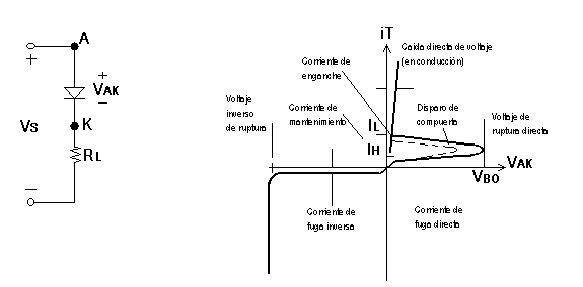
Once the tiristor is activated, it behaves as a diode in conduction and no longer is control on the device. The tiristor will continue leading, because in the J2 union a layer of exhaustion of life to free movements of carriers does not exist. Nevertheless if the direct current of the anode below a level known like current of maintenance IH is reduced, a region of exhaustion around the J2 union is generated due to the reduced number of carriers; the tiristor will be then in state of blockade. The maintenance current is of the order of the milliamperes and is minor who the enlistment current, IL. This means that IL>IH. The current of maintenance IH is the current of the minimum anode to maintain the tiristor in state of permanent regime. The maintenance current is minor who the enlistment current.
When the voltage of the cathode is positive with respect to the one of the anode, the J2 union has direct polarization, but the unions J1 and J3 have inverse polarization. This is similar to two diodes connected in series with an inverse voltage through them. The tiristor will be in inverse state of blockade and a current of inverse, well-known flight like current of inverse flight TO GO, will flow through the device.
MODEL OF TIRISTOR OF TWO TRANSITORES.
The regenerative action or of enlistment of life to the direct feedback can be demonstrated by means of a model of tiristor of two transistors. A tiristor can be considered like two complementary transistors, a transistor PNP, Q1, and a transistor NPN, Q2, so and as it is demonstrated in figure 3.
The current of collector IC of a tiristor is related, in general, with the current of the emitting IE and the current of flight of the union collector-bases ICBO, like
IC = IE + ICBO..........................(1)
The gain of current of common base is defined as = IC/IE. For the Q1 transistor the current of the emitter is the current of anode IA, and the current of collector IC1 can be determined from the equation (1):
IC1 = 1 IA + ICBO1........................... (2)
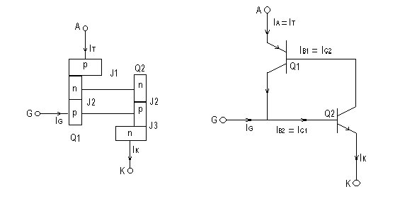
Where alfa1 is the gain of current and ICBO1 is the current of flight for Q1. In similar form for the Q2 transistor, the current of collector IC2 is:
IC2 = ÌK + ICBO2.............................. (3)
Where 2 are the gain of current and ICBO2 is the current of flight corresponding to Q2. When combining IC1 and IC2, we obtain:
IA = IC1 + IC2 = 1IA + ICBO1 + ÌK + ICBO2............................(4)
But for a current d equal floodgate AIG, IK=IA+IG solving the previous equation based on IA we obtain:
IA = 2 IG + ICBO1 + ICBO2...............................(5)
1 - ( 1 + 2)
ACTIVATION OF THE TIRISTOR
A tiristor activates increasing it current of the anode. This can be carried out by means of one of the following forms.
THERMAL. If the temperature of a tiristor is high will be an increase in the electron-hollow number of pairs, which will increase the currents of flight. This increase in the currents will cause that 1 and 2 increases. Due to the regenerative action ( 1+ 2) it can tend to the unit and the tiristor could activate. This type of activation can cause a thermal flight that generally is avoided.
LIGHT. If it is allowed that the light arrives at the unions of a tiristor, they increased the pairs electron-hollow being able to activate the tiristor. The activation of tiristores by light is obtained allowing that this arrives at silicon disks.
HIGH VOLTAGE. If the direct voltage cathode anode is greater than the direct voltage of rupture VBO, will flow a current of flight sufficient to initiate a regenerative activation. This type of activation can be destructive reason why it is due to avoid.
dv/dt. If the speed of elevation of the voltage anode-cathode is high, the current of load of the capacitivas unions can be sufficient to activate the tiristor. A high value of load current can damage the tiristor reason why the device must be protected against dv/dt high. The manufacturers specify dv/dt maximum permissible of the tiristores.
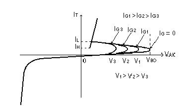
FLOODGATE CURRENT. If a tiristor is polarized in direct, the injection of a current of floodgate when applying a positive voltage of floodgate between the floodgate and the terminals of the cathode will activate to the tiristor. In agreement it increases the current of floodgate, is reduced the direct voltage of blockade, so and as it appears in fig.4
The tiristores make almost exclusively by diffusion. The current of the anode requires of a finite time to propagate by all the area of the union, from the point near the floodgate when it initiates the signal of the floodgate to activate the tiristor. In order to control di/dt, the time of activation and the time of decontamination, the manufacturers use several structures of floodgate.
Depending on the physical construction and the behavior of activation and decontamination, in general the tiristores can be classified in nine categories:
1. Tiristores of phase control (SCR).
2, Tiristores of fast commutation (SCR).
3, Tiristores of decontamination by floodgate (GTO).
4, Tiristores of bidirectional triode (TRIAC).
5, Tiristores of inverse conduction (RTC).
6, Tiristores of static induction (SITH).
7. Rectifiers controlled by silicon activated by light (LASCR)
8, Tiristores controlled by FET (FET-CTH)
9, Tiristores controlled by MOS (MCT)
In this it practices was necessary besides to use tiristores, the use of a special type of these as it is it a UJT in addition to a PUT reason why both are defined next:
MONOUNION TRANSISTOR (UJT).
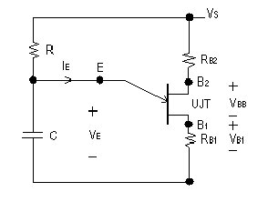
The transistor monounion (UJT) is used generally to generate firing signals in the SCR. In fig.5 is a basic circuit of firing UJT. A UJT has three terminals, well-known like emitter and, base1 B1 and base2 B2. Between B1 and B2 the monounion has the characteristics of an ordinary resistance (the resistance between bases RBB having values in the 9,1 rank of 4,7 and K). When the voltage of feeding versus in CD is applied, capacitor C through resistance R is loaded, since the emitting circuit of the UJT is in open state. The constant of time of the circuit of load is T1=RC. When the voltage of the emitter SEES, the same one that the voltage of the capacitor arrives at a value Vp tip, activates the UJT and the capacitor unloading through RB1 at a speed determined by the constant of time T2=RBÇ. T2 is much smaller than T1. When the voltage of the emitter SEES is reduced to the point of valley Vv, the emitter lets lead, the UJT is deactivated and the cycle of load is repeated.
The voltage of firing VB1 must design the sufficiently great thing like activating the SCR. The period of oscillation, T, is totally independent of the voltage of feeding versus and is given by:
T = 1/f = RC ln 1/1-n
TRANSISTOR PROGRAMMABLE MONOUNION.
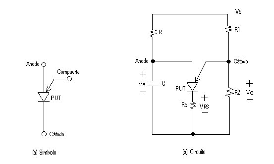
The transistor programmable monounion (PUT) is a small tiristor that appears in fig.7. A PUT can be used like a relaxation oscillator, so and as it is in fig.7b. The voltage of floodgate Vg stays from the feeding by means of the resistivo splitter of the voltage R1 and R2, and determines the voltage of point of Vp tip. In the case of the UJT, Vp he is fixed for a device by the voltage of feeding of CD, but in a PUT it can vary when modifying when modifying the value of resistivo splitter R! and R2. If the voltage of the anode GOES she is minor who the voltage of floodgate Vg, him device will be conserved in its inactive state, but if the anode voltage exceeds to the one floodgate in a fall voltage diode YOU, the tip point is reached and the device activates. The current of tip IP and the current of the valley point IV depend on the equivalent impedance in floodgate RG = R1R2/(R1+R2) and of the voltage of feeding in CD general versus N Rk Ohms is limited a value below 100.
R and Cs control the frequency R1 and R2 along with. The period of oscillation T is given in form approximated by:
T = 1/f = RC lnVs/Vs-Vp = RC ln (1+R2/R1)
TRIAC:
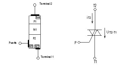
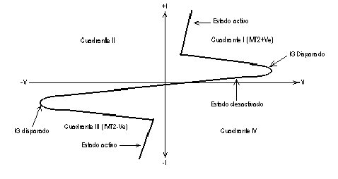
The TRIAC (conductive triode AC) is a semiconductor able to block tension and to lead current in both senses between the main terminals T1 and T2. Their basic structure and symbol appear in fig.8. It is a symmetrical component as far as conduction and state of blockade talks about, because the characteristic in quadrant I of curve UT2-T1 --- iT2 is equal to the one of quadrant III. It has flights in blockade and a practically equal fall of tension in conduction to those of a tiristor and the fact that between in conduction, if the tension of rupture in any sense is surpassed, it makes immune to destruction by surge.
EQUIVALENT CIRCUIT OF A TRIAC:
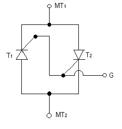
It is possible to be considered to a TRIAC as if were two SCR connected in antiparallel, with a connection of common floodgate, as it is in fig.9
Since the TRIAC is a bidirectional device, it is not possible to identify his terminals like anode and cathode. If terminal MT2 is positive with respect to terminal MT1, a negative signal to the floodgate will activate when applying, between the floodgate and terminal MT1.
It is not necessary that both polarities in the signals of the floodgate esten present and a TRIAC can be activated with a single positive or negative signal of floodgate. Actually, sensitivity varies from a quadrant to another one, the TRIAC normally operates in quadrant I (voltage and positive current of floodgate) or in quadrant III (voltage and negative current of floodgate).
WAYS OF OPERATION OF A TRIAC:
The TRIAC can be shot in anyone of two quadrants I and III by means of the application between the terminals door and T1 of a positive or negative impulse. This gives a facility him of great use and simplifies to much the firing circuit. Next the internal phenomena will be seen that they take place in the four possible ways of firing.
Way I +: Positive T2 terminal with respect to T1.
Intensity of incoming door.
Tiristor layers P1N1P2N2 as with emitter in short circuit work, since the bonding of the terminal of the cortocircuita cathode partially the emitting layer N2 with the P2.
The door current circulates internally until T1, partly by union P2N2 and partly through the P2 zone. The natural electron injection of N2 to P2 takes place that is favored in the area next to the door by the tension fall that produces in P2 the lateral circulation of door current. Part of injected electrons reaches about diffusion the union P2N1, that blocks the outer potential, and is accelerated by her beginning the conduction.
Way I -: Positive T2 terminal with respect to T1.
Intensity of salient door.
The firing is similar to the one of the tiristores of union door. Initially it leads auxiliary structure P1N1P2N3 and soon the main P1N1P2N2.
The firing of first takes place like a normal tiristor acted T1 of door and P of cathode. All the auxiliary structure is put to the positive tension of T2 and strongly polarizes the union P2N2 that injects electrons towards the area of positive potential. Union P2N1 of the main structure that supports the outer tension, is invaded by electrons in the vicinity of the auxiliary structure, entering conduction.
Way III +: Negative T2 terminal with respect to T1.
Intensity of incoming door.
The firing takes place by the called procedure of remote door. Structure P2N1P1N4 enters conduction.
The electron injection of N2 to P2 is equal to described in way I +. Those that reach about diffusion union P2N1 are absorbed by their potential of union, becoming more conductor. The positive potential of door more positively polarizes the area of union P2N1 next to her that next to T1, causing itself an injection of hollows from P2 to N1 that partly reaches union N1P1 in charge to block the outer tension and the entrance in conduction takes place.
Way III -: Negative T2 terminal with respect to T1.
Intensity of salient door.
Also one goes off by the procedure and remote door, leading layers P2N1P1N4.
The N3 layer injects electrons in P2 that make more conductor union P2N1. The positive tension of T1 more positively polarizes the next area of union P2N1 than the next one to the door. This polarization injects hollows of P2 to N1 that reach union N1P1 partly and they make it happen to conduction.
The four described ways of firing have different sensitivity. Being ways I + and III - most sensible, followed close by by the I -. way III + is the most difficult firing and must be avoided its use as far as possible.
The manufacturer facilitates data of electrical characteristics the blockade, conduction and of different by door of form similar to the explained thing for the tiristor.
 |
 |
 |
 |
||
| PRINCIPAL | ELECTRÓNICA | INFORMÁTICA | TECNOLOGÍA | ||
| Ciencias Místicas - www.cienciasmisticas.com.ar - El sitio de electrónica, informática y tecnología. | |||||